


联系人:莫长青
邮箱:774999923@qq.com
电话:13380799980
地址: 广东深圳市龙华区汇隆智造空间A503
| 品牌 |
斯瑞纳 |
型号 |
2090 |
| 货号 |
THR009 |
材质 |
树脂 |
| 加工定制 |
否 |
是否进口 |
否 |
| 产地 |
深圳 |
|
p2090a
20v, 3.2m惟, 90a, single n-channel
1.features
鈼? 20v mosfet technology
鈼? low on-state resistance
鈼? fast switching
鈼? vgs卤12v
2.applications
鈼? power switching application
鈼? load switching
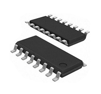
to-252
pin deion
vds
rds(on) typ.
id max.
20v
2.9m惟 @ 7.4v
90a
3.2m惟 @ 4.5v
3.7m惟 @ 2.5v
schematic diagram
3.absolute max ratings at ta=25鈩? (note1)
parameter
symbol
maximum
units
drain to source voltage
vdss
20
v
gate to source voltage
vgss
卤12
v
drain current (dc)
id
90
a
drain current (pulse), pw鈮?300渭s
idp
243
a
total dissipation
pd
83
w
avalanche energy, single pulsed
eas
260
mj
junction temperature
tj
150
鈩?
storage temperature
tstg
-55 to +150
鈩?
note 1: stresses exceeding those listed in the maximum ratings table may damage the device. if any of
these limits are exceeded, device functionality should not be assumed, damage may occur and reliability may
be affected.
4.thermal resistance ratings
parameter
symbol
value
unit
junction to case
r胃jc
1.8
鈩?/w
note 2锛歐hen mounted on 1 inch square copper board t 鈮? 10sec the value in any given application depends
on the user&锛?39;s specific board design.
d
g
s
rev.1.2 wan semnductor (ningbo) co.,ltd 2
wp2090a
5.electrical characteristics at ta=25鈩? (note 3)
parameter
symbol
test conditions
min.
typ.
max.
units
drain to source breakdown voltage
v(br)dss
id = 250渭a, vgs = 0v
20
v
zero-gate voltage drain current
idss
vds = 20v, vgs = 0v
1
渭a
gate to source leakage current
igss
vgs = 卤12v, vds = 0v
卤100
na
gate threshold voltage
vgs(th)
vds=vgs, ids=250渭a
0.5
0.75
1.2
v
static drain to source on-state
resistance
rds(on)
id = 30a, vgs = 7.4v
-
2.9
3.7
m惟
id = 20a, vgs = 4.5v
-
3.2
3.9
m惟
id = 20a, vgs = 2.5v
-
3.7
6.1
m惟
forward transconductance
gfs
id = 20a, vds = 5v
20
s
input capacitance
ciss
vgs=0v,
vds=10v,
frequency=1.0mhz
2016
pf
output capacitance
coss
391
pf
reverse transfer capacitance
crss
130
pf
turn-on delay time
td(on)
vdd = 10v, id = 20a,
vgs = 10v,
rgen = 2.7惟
6
ns
rise time
tr
4
ns
turn-off delay time
td(off)
31
ns
fall time
tf
5
ns
total gate charge
qg
vds = 10v,
vgs = 4.5v,
id = 20a
15
nc
qgs
3
nc
qgd
4
nc
diode forward voltage
vfsd
is = 20a, vgs = 0
1.2
v
note 3锛歅roduct parametric performance is indicated in the electrical characteristics for the listed test
conditions, unless otherwise noted. product performance may not be indicated by the electrical
characteristics if operated under different conditions.
rev.1.2 wan semnductor (ningbo) co.,ltd 3
wp2090a
6.typical electrical and thermal characteristics
output characteristics transfer characteristics
rdson-drain current rdson-junction temperature
gate charge source-drain diode forward
rev.1.2 wan semnductor (ningbo) co.,ltd 4
wp2090a
capacitance vs vds safe operation area
bvdss vs junction temperature vgs(th) vs junction temperature
normalized maximum transient thermal impedance
rev.1.2 wan semnductor (ningbo) co.,ltd 5
wp2090a
7.package dimensions
rev.1.2 wan semnductor (ningbo) co.,ltd 6
wp2090a
8. important notice
wan semnductor (ningbo) co.,ltd reserves the right to make corrections, enhancements,
improvements and other changes to its semiconductor products and services and to discontinue any product
or service. buyers should obtain the latest relevant information before placing orders and should verify that
such information is current and complete. all semiconductor products (also referred to herein as
鈥渃omponents鈥?) are sold subject to wansemi鈥檚 terms and conditions of sale supplied at the time of order
acknowledgment.
wansemi warrants performance of its components to the specifications applicable at the time of sale, in
accordance with the warranty in wansemi鈥檚 terms and conditions of sale of semiconductor products. testing
and other quality control techniques are used to the extent wansemi deems necessary to support this
warranty. except where mandated by applicable law, testing of all parameters of each component is not
necessarily performed.
wansemi assumes no liability for applications assistance or the design of buyers鈥? products. buyers are
responsible for their products and applications using wansemi components. to minimize the risks
associated with buyers鈥? products and applications, buyers should provide adequate design and operating
safeguards.
no wansemi components are authorized for use in fda class iii (or similar life-critical medical
equipment) unless authorized officers of the parties have executed a special agreement specifically governing
such use.
unless wansemi has specifically designated certain components which meet iso/ts16949
requirements, mainly for automotive use, wansemi will not be responsible for any


 13380799980